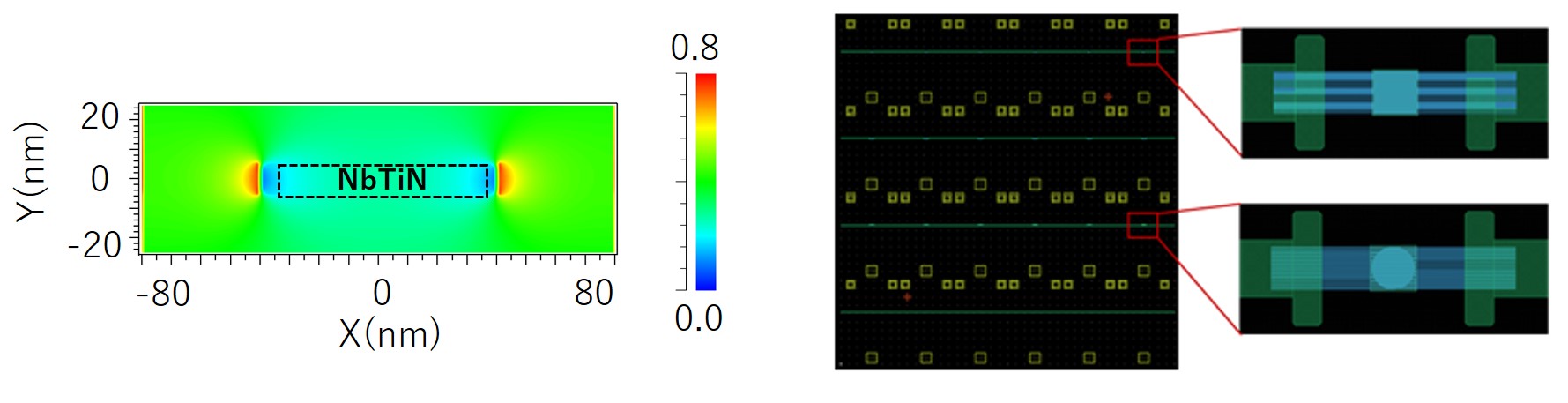
- Device design ・The device structure that provides high performance is studied by simulating the electric field distribution inside the device using the finite-difference time-domain (FDTD) method.
- Thin film growth ・Si wafers are cut, cleaned, and thermally oxidized to produce substrates for thin film growth.
- Microfabrication ・The thin film is processed into micron-wide strips by photolithography and dry etching, etc.
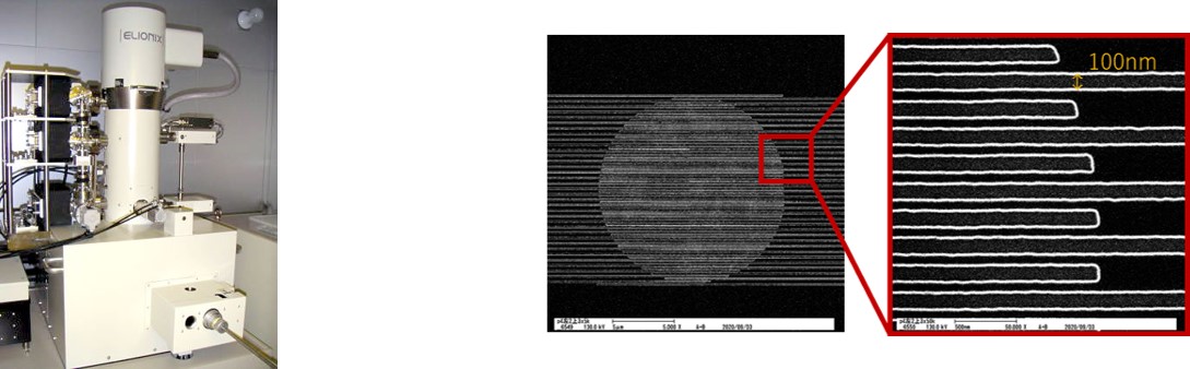
- Nanofabrication ・If nanofabrication is required, master's students will use Hokkaido University's nanotechnology equipment to perform nanometer-sized fabrication.
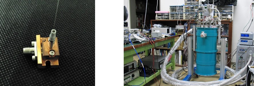
- Characterization ・Mount the device in a holder and align the optical fiber with the light-collecting position under the microscope.
・Create the device drawing with CAD software.
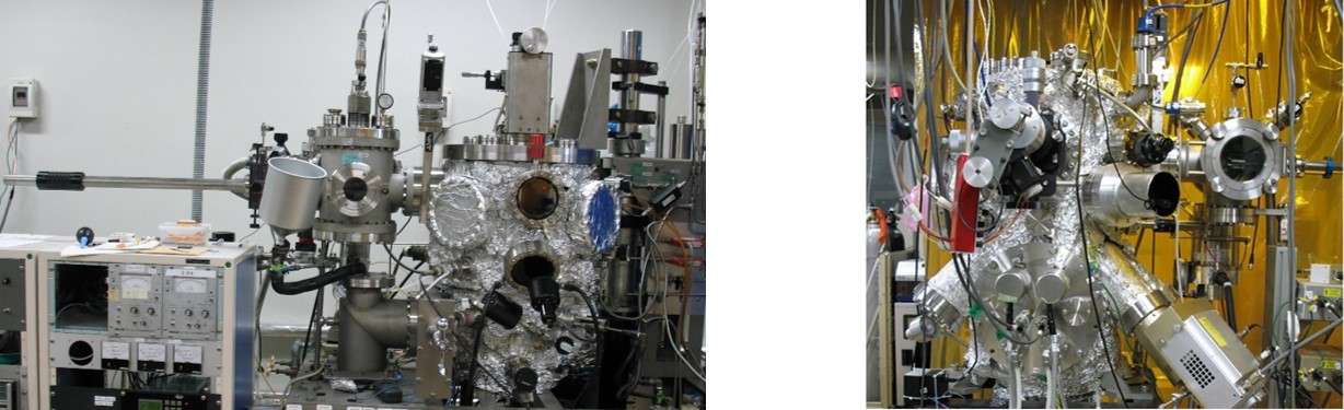
・Superconducting thin films are grown using sputtering or MBE thin film growth equipment.
・Evaluate thin film properties by X-ray diffraction and resistivity measurements.
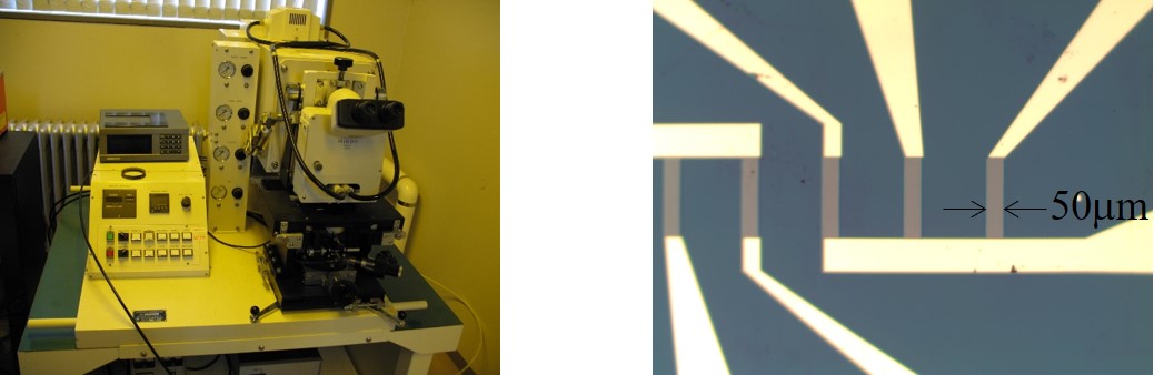
・Electrodes are fabricated by photolithography and gold vapor deposition, etc.
・The wafer is cut into individual chips by dicing.
・Cool the device and measure the electrical conductivity properties of the device such as I-V characteristics.
・A device is irradiated with extrimely weak laser light through an optical fiber, and optical device characteristics such as quantum efficiency, dark count rate, and jitter are measured.